Quantum and Carbon Nanomaterials
NREL remains at the forefront of quantum and carbon nanomaterials research, expanding into a broader effort that includes layered semiconducting and thermoelectric materials.
We aim our efforts at:
- Understanding the fundamental properties of quantum and carbon nanomaterials
- Tuning and controlling their optical and electronic properties
- Using these materials in thermoelectrics, photovoltaics, water splitting, hydrogen storage, batteries, and transistors.
Quantum and carbon nanomaterials activities are funded by the U.S. Department of Energy Office of Basic Energy Science and commercial partners.
Capabilities
In-House Material Synthesis and Purification
- Temperature-controlled pulsed laser vaporization of a graphite target for single-walled carbon nanotubes (SWCNT) synthesis
- Designer SWCNT syntheses, such as 13C-labeled, boron-doped, nitrogen-doped
- Arc discharge system for large-diameter SWCNT synthesis
- Multiple chemical vapor deposition (CVD) systems for synthesis of SWCNTs, graphene, or monolayer transition-metal dichalcogenides (TMDCs)
- Mechanical exfoliation of SWCNTs using ultrasonic tip or shear-force mixer
- Solution-phase chemical exfoliation of TMDCs
- Ultracentrifuge for purifying and separating exfoliated SWCNTs or TMDCs
Suite of Spectroscopic and Surface/Structural Characterization Tools
- Spectroscopic systems capable of steady-state and time-resolved spectroscopic characterization of nanoscale materials, spanning wavelengths from the ultraviolet to mid-infrared
- Surface characterization tools: X-ray photoelectron spectroscopy, Auger spectroscopy, transmission electron microscope, scanning tunneling spectroscopy and microscopy, scanning Kelvin probe microscopy, X-ray diffraction, and others
- In-situ growth characterization tools: including low-energy electron diffraction, reflection high-energy electron diffraction, and spectroscopic ellipsometry.

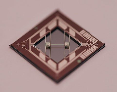
This thin-film transport measurement system is based on an ultra-thin suspended SiN bridge.
Transport Property Measurement Systems
We have a wide array of thermoelectric characterization capabilities, including a physical properties measurement system, a homebuilt method-of-four-coefficients system, and a thin-film transport measurement system based on an ultra-thin suspended silicon nitride bridge.
Carbon Nanoscience Research
We study the fundamental properties and applications of low-dimensional carbon-based materials, including single-walled carbon nanotubes and graphene.

Vials of SWCNTs that are separated by electronic structure. The diameter-dependent optical absorption produces tunable colors for these dispersions.
Single-Walled Carbon Nanotubes
SWCNTs are cylindrical nanomaterials composed of a single sheet of sp2-bonded carbon rolled into a tube with a large aspect ratio. The diameter of commonly
synthesized SWCNTs ranges from about 0.7 to 2 nm, whereas the length can exceed tens
of microns. SWCNTs can have either a semiconducting or metallic electronic structure,
and the statistical ratio of most as-synthesized samples is 2:1 semiconducting:metallic.
We explore the fundamental chemistry and physics of SWCNTs as well as incorporate
SWCNTs into high-performance energy-conversion applications. We synthesize our own
SWCNTs in-house by techniques such as laser vaporization, arc discharge, and CVD.
We also develop and use numerous methods for separating SWCNTs by electronic structure,
diameter, and chiral angle, including: density gradient ultracentrifugation, aqueous
two-phase extraction, and selective extraction with conjugated polymers. We develop
and research a number of novel energy conversion materials and technologies based
on SWCNTs, including thin-film photovoltaics, catalytic electrodes, battery electrodes,
and thermoelectric materials.

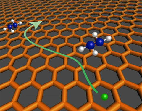
Illustration of charge transport within a chemically doped graphene thin film.
Graphene
Graphene is a one-atom-thick, two-dimensional, semi-metallic material composed entirely
of sp2-bonded carbon. Graphene's extremely high conductivity and optical transparency make
it a relevant material for several interesting renewable energy applications.
We synthesize monolayer graphene by CVD and also synthesize colloidal graphene by
exfoliation of graphite. We examine the fundamental transport properties of graphene,
and the use of graphene in novel energy-conversion technologies, such as transparent
conducting electrodes for thin-film solar cells and interfacial layers in technologies
such as smart windows.
Layered Semiconductors Research
We study the fundamental properties and applications of quantum-confined layered materials, including TMDCs.

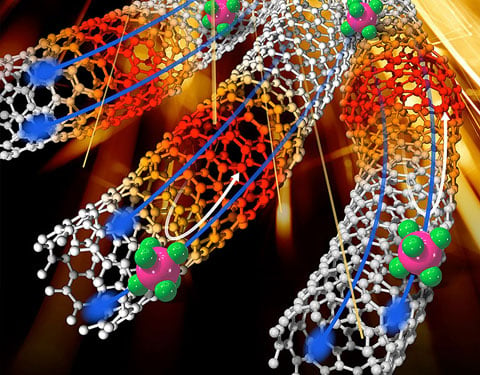
Functional organic thermoelectric composites can be improved with carbon nanotube inclusions.
A number of two-dimensional, layered semiconductors with variable electronic structure
(semiconducting to metallic) provide an interesting counterpoint to graphene. One
popular class of such materials—TMDCs (MoS2, MoSe2, WS2, and WSe2)—has gained increasing interest in the research community in recent years. The properties
of TMDCs can change abruptly from those of the bulk material when the semiconductor
is grown, or exfoliated, as a single monolayer.
We are interested in the fundamental photophysics of layered 2-D semiconductors, and
how these properties change as a function of external stimuli (e.g., stress, strain,
functionalization, doping). Another area of active research is understanding and manipulating
surfaces and interfaces to control charge dynamics between the TMDCs and substrates
or between TMDCs and solution. We synthesize TMDCs by either CVD or chemical exfoliation
and are interested in how the optical and electrical properties of these interesting
materials influence their behavior in applications such as thin-film photovoltaics,
energy storage, and catalytic electrodes for hydrogen evolution.
Thermoelectric Materials Research

Functional organic thermoelectric composites can be improved with carbon nanotube inclusions.
Thermoelectric devices directly convert temperature differences and electric voltage, allowing electricity generation from waste heat (via the Seebeck effect) or local cooling/heating (via the Peltier effect). The efficiency of thermoelectric electricity generation is related to the active material's electrical conductivity (σ), Seebeck coefficient (α), and thermal conductivity (κ), and it is typically captured in a figure of merit (zT) at a given temperature (T):

whereas the Peltier coefficient (Π) is directly related to the Seebeck coefficient (α) at a given temperature (T):
![]()
Because the three material properties (σ, α, and κ) are inter-related, a primary goal of thermoelectrics research is the rational control of the carrier density and interfaces within a material to optimize zT.
We develop and study thermoelectric materials primarily with a bottom-up approach, using nanomaterial building blocks to design and control the nano- and meso-scale morphology and interfaces of complex thermoelectric materials. Some of the material systems we explore include single-walled carbon nanotubes, semiconducting polymers, semiconductor nanocrystal arrays, and composite materials including some combination of these building blocks. The goal of our approach is to use nanoscale interfaces to increase α and decrease κ while maintaining high σ.
Research Highlights
As-produced SWCNTs typically come as a mixture of semiconducting and metallic species, in a statistical ratio of 2:1, and they are often contaminated with amorphous carbon, fullerenes, and metallic catalyst impurities. To simplify studies of their fundamental properties and to improve their function in various applications, we have developed a variety of approaches to remove the impurities and to enrich the sample in target species. These approaches include density gradient ultracentrifugation, aqueous two-phase extraction, and selective extraction with conjugated polymers. By carefully tuning the processing conditions, these techniques are capable of separating SWCNTs by diameter, end-capped (empty endohedral volume) vs. open-ended (endohedral volume filled with solvent/dye molecules), and electronic character (semiconducting vs. metallic), and can even produce samples highly enriched in a few or single SWCNT chiral species.
We use a suite of spectroscopic techniques to probe the fate of excitons and charge carriers in interfaces between SWCNTs and other semiconductor materials. Early work explored the ability of SWCNTs to act as energy and/or charge-carrier acceptors in composites with thiophene-based conjugated polymers, ultimately determining that the free-carrier lifetime is limited by the presence of metallic SWCNTs. As the strategies described above to enrich semiconducting SWCNTs matured, our attention turned toward their potential as light-harvesting components in their own right. Initial studies confirmed the ability of the s-SWCNT-C60 fullerene bilayer interface to efficiently dissociate excitons and spatially separate long-lived free carriers, but pointed toward a dependence of the free-carrier yield on the energetic driving force at the interface. By tuning the electron affinity of the fullerene-derivative acceptor layer, we were able to identify the optimum energetic driving force for free-carrier generation for s-SWCNTs with quite different electronic bandgaps.
The unique optical properties (strong, tunable absorption bands) and electronic properties (excellent charge transport) of SWCNTs make them attractive as both light-harvesting active layers and selective charge-extraction layers in photovoltaic applications. Initial efforts sought to employ ultrasonically sprayed SWCNT networks as a replacement for indium-doped tin oxide as the transparent conducting electrode in organic photovoltaic devices. This approach was extended to also replace the poly(3,4-ethylenedioxythiophene):poly(styrene-sulfonate) (PEDOT:PSS) hole transport layer, which is highly corrosive and can lead to device instability. More recently, we have employed highly enriched semiconducting SWCNTs as an efficient interfacial hole extraction layer in high-performance methyl ammonium lead iodide (MAPbI3) perovskite photovoltaics. Finally, we have demonstrated organic photovoltaic devices approaching 1% power conversion efficiency that employ near-monochiral (7,5) SWCNTs as the primary light-harvesting component.
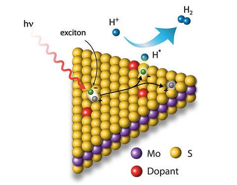
We show that the 2D-MoS2 surface energetics and stability can be controlled by chemical modification of the surface via organic molecules with varying electronic properties. Chemically exfoliated, metallic MoS2 is modified with substituted phenyl rings containing substituents with various electron withdrawing/donating groups. This functionalization results in different electrochemical properties—specifically, activity toward the hydrogen evolution reaction. In addition, the workfunction of the metallic MoS2 surface depends on the functional group, and it correlates with the electron withdrawing/donating character (Hammett parameter) of the functional group. The shallower the workfunction of modified MoS2, the better the functionalized MoS2 is for hydrogen evolution reaction. Furthermore, the metallic nature of the MoS2 films are preserved by the functional group and do not undergo conversion to the thermodynamically stable semiconducting state. Functionalizing 2D TMDCs gives an extra handle on electronic properties and stability within the typically unstable metallic state.
Contacts
The Chemistry and Nanoscience Center is part of the Materials, Chemical, and Computational Science directorate, led by Associate Laboratory Director Bill Tumas.
Share
Last Updated May 19, 2025
