Into Another Dimension: Nanoscale Trilayer Exhibits Ultrafast Charge Transfer in Semiconductor Materials

Successfully innovating optoelectronic semiconductor devices depends a lot on moving charges and excitons—electron-hole pairs—in specified directions for the purpose of creating fuels or electricity.
In photosynthesis, pigment molecules absorb and transfer solar energy to a reaction center, where the energy is converted and used. As this process occurs, photons generate electron-hole pairs that must be separated to initiate chemical reactions.
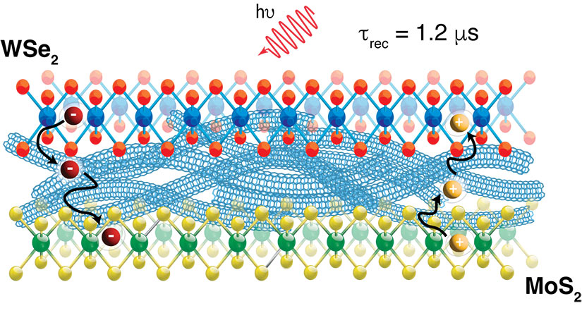
Deriving inspiration from the natural process of photosynthesis, National Renewable Energy Laboratory (NREL) researchers developed a mixed-dimensionality (2D/1D/2D) trilayer of semiconductors to enable exciton dissociation. This exciton dissociation step, a splitting and spatial separation of excited electron–hole pairs, is a microscopic process that is fundamental to the performance of photovoltaic systems. Researchers detailed the findings in “Ultrafast Charge Transfer Cascade in a Mixed-Dimensionality Nanoscale Trilayer,” published in ACS Nano.
As the clean energy transition progresses, advances in photovoltaic systems, which convert sunlight into electricity, are crucial. Photovoltaics rely on the light-activated creation of separated electron-hole pairs to drive an external circuit.
“In this study, we were able to create light-activated electron hole pairs and separate them for a long time, longer than previously reported similar systems,” said NREL’s Alexis Myers, a graduate student researcher.
Low-Dimensional Materials Present Opportunities for Exciton Transfer Study
The diverse and tunable electronic and optical properties of quantum-confined low-dimensional materials such as two-dimensional (2D) transition metal dichalcogenides (TMDCs) and one-dimensional (1D) single-walled carbon nanotubes (SWCNTs) make them prime candidates for fundamental studies on charge and exciton transfer. These types of materials have enhanced electron-hole Coulomb interactions, where the electrostatic force causes the attraction between an electron and an electron hole to form an exciton. To separate the charges, researchers must overcome the attraction, made more difficult by the large binding energies.
These materials exhibit large exciton binding energies—the energy needed for exciton dissociation—which can inhibit generation of electrical currents for photovoltaics, photodetectors, and sensors or chemical bonds in solar fuel schemes. So, NREL researchers sought to develop a hetero-trilayer that would address this challenge.
“Extending charge separation lifetimes is necessary to increase the chance of charge extraction,” Myers said. “The creation of bilayers and trilayers comes from this desire to increase the distance between separated charges. However, it’s unclear in the literature whether the ‘separated’ charges are still electrostatically bound across the interface. So, though separated, the Coulomb interaction is still present, which can decrease charge separation lifetimes. In the trilayer, we were able to track the movements of electrons and holes sequentially through each layer, confirming they are indeed no longer bound to each other.”
Lengthening Charge Separation Lifetimes Enables Better Electric Current Generation
Complex, low-dimensional heterostructures—like TMDCs—exhibit longer lifetimes, initiating important photochemical reactions, which are critical to generating electricity in photovoltaics. Alexis Myers and team developed a mixed-dimensionality hetero-trilayer of SWCNTs between two semiconductors that enables a photoinduced charge transfer cascade where electrons (negative charge carriers) move in one direction while holes (positive charge carriers) move in the other direction.
The hetero-trilayer mimics the natural charge transfer cascade observed in plant photosynthesis, which inspired its development. A key part of the heterostructure is the one-dimensional middle layer, which helps the charge carriers diffuse efficiently from one 2D layer to the other.
The study also looked at the mechanics of carrier diffusion in TMDCs. Using transient absorption spectroscopy, researchers tracked exciton dissociation and charge diffusion across the hetero-trilayer, observing ultrafast electron transfer to one layer and hole transfer to the another. The trilayer architecture appears to facilitate ultrafast hole transfer and exciton dissociation, resulting in a long-lived charge separation.
The charge transfer cascade enables an excited state—where electrons and holes reside in separate places within the trilayer—where photochemical reactions could be initiated. Longer charge separation lifetimes could mean greater electric current generation because more electrons and holes have not recombined.
The trilayer produced double the carrier yield compared with a 2D/1D bilayer. It also empowered the separated charges to overcome the interlayer exciton binding energies of unbound separated charges, a key challenge with such materials.
"These materials have high electrostatic interaction between the electron and hole, yet we have shown that we can successfully separate them through efficient diffusion along the SWCNT mesh,” said NREL’s Alejandra Hermosilla Palacios, a materials science postdoctoral researcher. “Kinetic analysis of the different steps is necessary to understand the efficiency in these systems. We have mostly focused on the diffusion of charges thanks to the SWCNTs. We would like to understand how charges diffuse or move in the TMDC layer to better propose new systems that could lead to higher efficiencies—more electrons and holes generated—and even longer-lived charges (chance for higher electric current generation).”
In previous charge transfer cascades, the mechanism for charge transfer is unclear or does not proceed as expected.
“Our results suggest that well-defined charge transfer cascades can result in longer charge separated lifetimes and higher charge yield (or efficient transfer), paving the way for better understanding of how charges are moving through these systems and how we can continue to optimize them,” Myers said.
Further Studies—Future Innovation
The study results position these nanoscale models for further fundamental studies of the mechanics of carrier dynamics. The enhanced charge carrier yield suggests future applications in advanced optoelectronic systems. “The goal is to continue deconvoluting each step of the photovoltaic process to advance optimization,” Myers said.
“Our results show promising implications for the development of nanoscale optoelectronic devices like solar cells and solar fuel architectures,” Hermosilla Palacios said. “Mixed-dimensionality heterostructures demonstrate photophysics and technological advantages that may enhance and accelerate innovation in optoelectronics.”
Learn more about basic energy sciences at NREL and about the U.S. Department of Energy Office of Science Basic Energy Sciences Program. Read “Ultrafast Charge Transfer Cascade in a Mixed-Dimensionality Nanoscale Trilayer” in ACS Nano.

