Perovskite Solar Cells
NREL's applied perovskite program seeks to make perovskite solar cells a viable technology by removing barriers to commercialization by increasing efficiency, controlling stability, and enabling scaling.
Perovskite materials offer excellent light absorption, charge-carrier mobilities, and lifetimes, resulting in high device efficiencies with opportunities to realize a low-cost, industry-scalable technology. Achieving this potential will require us to overcome barriers related to stability and environmental compatibility, but if these concerns are addressed, perovskite-based technology holds transformational potential for rapid terawatt-scale solar deployment. The basic materials properties have also sparked interest in using hybrid perovskite semiconductors in a broader class of energy applications that span traditional electronic and optical systems.
In a few short years, NREL has made significant technical contributions to perovskite research, as demonstrated by its field-leading publications and significant interest by industry. NREL's impact has been enabled by short-term Laboratory Directed Research and Development funding and early investments from the Department of Energy's Office of Science, Office of Basic Energy Sciences, Solar Photochemistry Program, followed by efforts funded by the Department of Energy's Office of Energy Efficiency and Renewable Energy that focused on photovoltaics (PV).

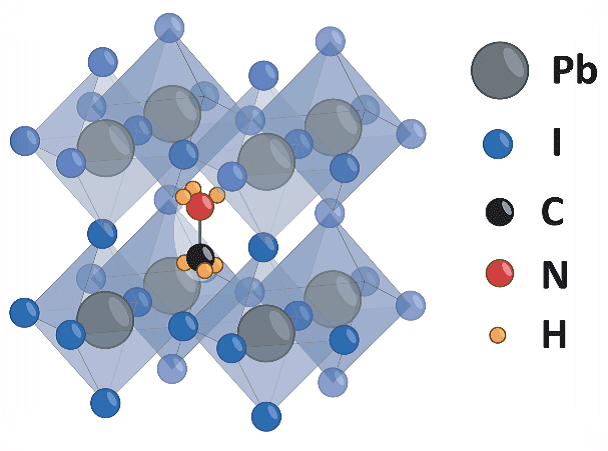
Methyl ammonium lead triiodide (CH3NH3)PbI3, or MAPbI3, is one of the perovskites we are exploring.
Our Expertise
We have perovskite PV expertise in:
- Basic materials characterization
- Fundamental photophysics, photochemistry, and exciton/charge-carrier dynamics
- Interfacial energy alignment and charge-transfer (carrier-collection) processes
- Structural and composition characterization
- Material and compositional engineering for improved stability
- High-efficiency solar cell fabrication with device performance and stability testing
- Scale-up, printing, slot-die coating, and roll-to-roll manufacturing.
Research Areas
The unique properties of halide perovskite systems and their ability to be solution-processed can enable their use—and, by proxy, NREL activities—in solution processing and advanced manufacturing.
The application space for this general class of systems includes low-power electronics, light emitters, detectors, and associated integrated-circuit systems for dynamic energy management with numerous applications.
The unique carrier cooling dynamics indicate that these systems may also be compelling for thermoelectric and associated energy-scavenging applications that cut across civilian and military energy needs.
Tools and Capabilities
NREL offers a range of tools and capabilities for R&D in perovskite materials and devices.
Materials and Device Construction
- Chemical synthesis and nanomaterial synthesis
The synthesis of novel precursors enables new perovskites or highly stable materials and nanocrystal starting materials for high-quality perovskite absorber layers. - State-of-the-art device fabrication
NREL regularly attains efficiencies of >20% and has high-efficiency devices at 1 cm2 and larger. - State-of-the-art synthesis of carbon nanotube contact materials
- Scale-up and large-area device fabrication
Facilities range from inkjet deposition within the atmospheric processing platform.
Materials and Device Characterization
- Femtosecond photoluminescence, transient absorbance, and transient terahertz spectroscopies
These techniques allow us to study the dynamics of excitons and charge carriers and to study charge transfer at interfaces. - Transient microwave conductivity
This unique tool is extraordinarily sensitive to free charge carriers and allows for the very sensitive study of carrier generation and charge transfer at solar-relevant light intensities. - Structure characterization using X-ray diffraction
Our facilities allow for large-scale combinatorial analysis of structure evolution during processing of perovskites. We also collaborate extensively with SLAC for this purpose.

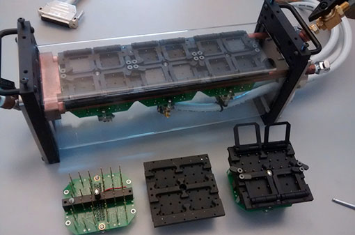
One test unit of the solar parameter analysis system can enable the simultaneous study of 12 1"-by-1" devices.
- Solar parameter analysis system
This system enables a unique suite of long-term reliability characterizations on individual PV cells. The system has four components: a flow cell; individually addressable, matrixed electrical channels for devices under test; a series of sensors/sensor channels; and control/measurement electronics. In addition to PV applications, the system can be applied to solid-state lighting, testing of coatings and barriers, batteries, and more. - Microscopy-based materials and device characterization
The perovskite effort also takes advantage of a comprehensive set of microscopy capabilities (e.g., scanning probe microscopies, transmission electron microscopy, and cathodoluminescence). These tools provide structural and electronic material information and can also give device-level insight into the electric fields with perovskite-based PV systems. (See use of cathodoluminescence; low-energy electron microscopy, electron energy-loss spectroscopy; in-situ transmission electron microscopy and X-ray diffraction; Kelvin probe force microscopy.) - Surface and interface characterization
Critical to understanding perovskite materials and devices are their interfaces with traditional electronic materials. Our perovskite effort uses a comprehensive suite of surface and interface characterization tools, which includes surface science capabilities (e.g., Auger electron spectroscopy, X-ray photoelectron spectroscopy, secondary ion mass spectrometry) as well as Department of Energy user facilities. (See use of photoemission spectroscopy/transient absorbance spectroscopy, X-ray and ultraviolet photoelectron spectroscopy.) - Solar simulator with current-voltage
- External quantum efficiency and flash/mapping external quantum efficiency
- Ultraviolet-visible spectrophotometer
- Surface profiler
- Optical microscopes
- Contact-angle setup
Projects
A history of our funded research in perovskites includes the following:
Laboratory Directed Research and Development
FY 2014–FY 2015
NREL's first funded perovskite-based project geared toward understanding the fundamental
nature of the device structure. This project initiated much of our present program.
NEXT Gen III
FY 2015–FY 2018
Focus was on developing high-efficiency multijunction perovskite-based solar cells. Key challenges included developing lower-bandgap perovskite material and tunnel junctions to connect the subcells in series.
Laboratory Directed Research and Development
FY 2015–FY 2016
In collaboration with SLAC, our goals were to understand high-level crystallography
and defects and their relation to device operation.
Directors Initiative Annual Operating Plan
FY 2015
Seed funds were used to develop the Office of Energy Efficiency and Renewable Energy SunShot National Laboratory Multiyear Program by enabling research activities prior to proposal submission.
Office of Basic Energy Sciences
The Solar Photochemistry core program is interested in fundamental aspects of solar photoconversion, including excitonic effects, charge transport, and charge transfer between layers. Perovskites are only a small part of the Basic Energy Sciences program; however, expertise developed within the program related to carbon nanotube contact layers, microwave conductivity, and carrier dynamics are applied to perovskite systems.
Office of Basic Energy Sciences
NREL's Center for Next Generation Materials by Design Energy Frontier Research Center
has looked into alternative lead-free perovskite materials and studied the electronic
properties that enable the lead-halide perovskite to be so effective. The Center for
Next Generation Materials by Design identified a class of materials, such as BiI3,
that mimic the perovskite's electronic structure.
Companies interested in NREL's expertise have established a partner relationship with NREL staff to help drive company research toward commercialization.
Completed in FY 2016, this project was extremely useful in establishing the experimental conditions to look successfully at these materials. It also informed device-level work with insight into fundamental aspects of the material microstructure during formation.
Annual Operating Plan
FY 2016–FY 2018
Funded by the Office of Energy Efficiency and Renewable Energy's SuNLaMP , this project focused on understanding materials problems, applications, and device configurations that may prevent or enable perovskite systems in energy-harvesting applications.
Topic 7
FY 2016
The goal was to develop new, highly stable perovskite materials by vapor deposition.
Details of three additional projects being conducted within the hybrid perovskite solar cells area are provided below.
Ultrahigh-Efficiency and Low-Cost Polycrystalline Halide Perovskite Thin-Film Solar Cells
| Au | ARC |
| Contact | |
| p-Perovskite (T) Window (~1018cm-3) | |
| p-Perovskite (T) Emitter (~1018cm-3) | |
| n-Perovskite (T) Base (~1017cm-3) | |
| n-Perovskite (T) BSF (~1018cm-3) | |
| Tunnel Junction | |
| p-Perovskite (B) Window (~1018cm-3) | |
| p-Perovskite (B) Emitter (~1018cm-3) | |
| n-Perovskite (B) Base (~1017cm-3) | |
| n-Perovskite (B) BSF (~1018cm-3) | |
| Metal | |
| Glass | |

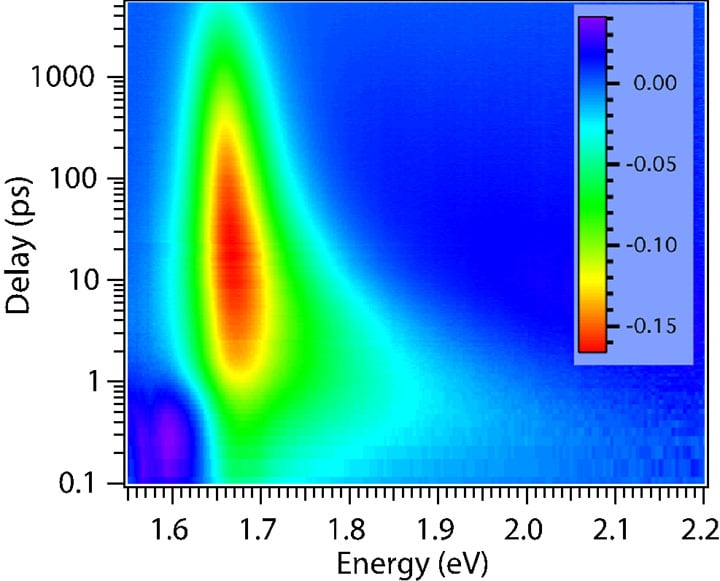
Very slow cooling of hot carriers in organic metal halide perovskite (see article).
We are developing dual-junction thin-film tandem solar cells using low-cost polycrystalline halide perovskites (e.g., CH3NH3PbI3) for both top and bottom cells. Halide perovskites have demonstrated exceptional progress in PV cell performance—from 3.8% in 2009 to a certified 22% in 2016. Remarkably, such high-efficiency perovskite solar cells can be made from polycrystalline materials by solution processing.
We want to:
- Understand basic material (e.g., doping and defect) and device properties related to halide perovskites
- Fabricate high-efficiency single-junction perovskite (top and bottom) cells
- Demonstrate ultra-high-efficiency tandem perovskite solar cells.
Our focus is on single-junction cells, using two complementary methods (solution and evaporation), trying to understand doping/defect physics and applying a tunnel junction or recombination layer for tandem cells. The figure shows a schematic of the cell architecture we are working on.
Ultrafast Dynamics of Charge Carriers in Organic Metal Halide Perovskites
We have extensively studied the ultrafast dynamics of excited states, including excitons and charge carriers and their recombination statistics.
- Ultraslow carrier cooling
NREL demonstrated that when excited with high-energy light, the charge carrier cooling rate in the perovskite material slows down during the cooling process—the slowed cooling observed in PbMAI3 is much slower than that found in traditional inorganic semiconductors and comparable to expensive, engineered multilayer quantum well structures—making this material a possible candidate for next-generation hot-carrier solar cells that can reach very high power conversion efficiencies. - Excitons impact optical absorption and recombination dynamics
Even though excitons are not stable at room temperature, the Coulomb interaction between electrons and holes impacts the optical absorption in these materials, increasing absorbance strength above GaAs and other prototypical semiconductors. We also found that the presence of excitons impacts recombination dynamics. - Very slow surface recombination
Using a novel ultrafast technique—transient photoreflectance spectroscopy—we found that even on unpassivated surfaces, surface recombination is very slow in these materials, much slower than surface recombination on other (unpassivated) semiconductors.
Electronic Energy Level Alignment at the Carbon Nanotube/Organic Metal Halide Perovskite Interface
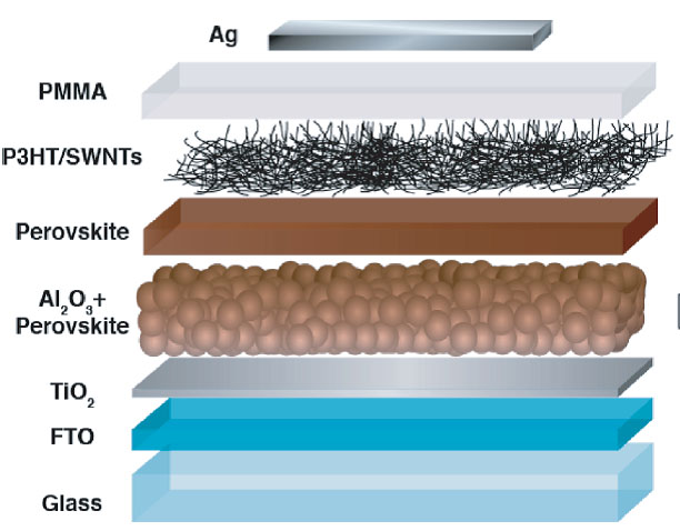
Printed carbon contacts can be implemented as a charge-carrier transport layer alternative to conventional organic or oxide transport layers. We are demonstrating that devices with carbon nanotubes embedded in a polymer matrix can yield high efficiencies and improved stability. The carbon nanotubes processing is compatible with scaling approaches via spray coating and printing techniques. See "Efficient Charge Extraction and Slow Recombination in Organic–Inorganic Perovskites Capped with Semiconducting Single-Walled Carbon Nanotubes" for more information.

- Quantify interface energetics
We are using photoemission spectroscopy on thin single-walled carbon nanotube (SWCNT) layers and probing surface sensitivity to study electronic interaction and chemical changes. We are also tracking band bending in methylamine lead iodide (MAPbI3) films as a function of SWCNT overlayer thickness. - Interface electronic structure
We are determining valence-band structure from ultraviolet photoemission spectra. One result is band bending in a SWCNT layer with n-type SWCNT at the MAPbI3/SWCNT interface to a slightly p-type SWCNT film further away from the interface. - Interface chemistry
We are using X-ray photoemission spectroscopy and find no band bending in MAPbI3. SWCNT core-level shifts track with band bending observed in valence-band spectra. - Ground-state charge transfer
We have found electron donation from methyl ammonium to SWCNT, so that SWCNT becomes n-type at the interface subsequent to band bending in SWCNT to an intrinsic state. A SWCNT overlayer causes no band bending in the MAPbI3 film, and there is no barrier for hole collection at the interface, so there is rapid and efficient hole extraction. Band bending in SWCNT is ideal for shuttling holes to the cell terminal. - Charge-carrier extraction
We use transient absorption spectroscopy to track charge-carrier dynamics and note rapid charge-carrier extraction.
Contact
Senior Scientist, Perovskite and Hybrid Solar Cells Team Lead
Share
Last Updated April 3, 2025
