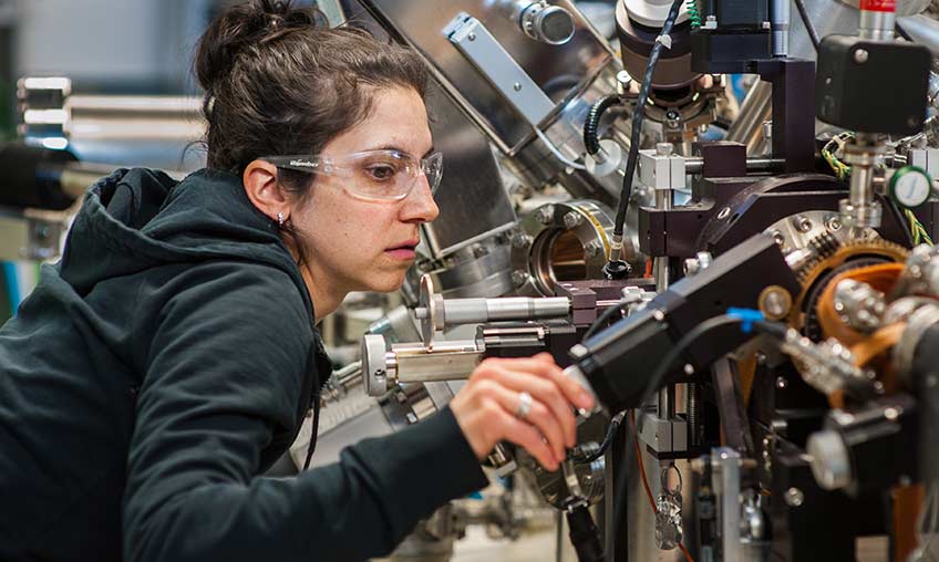
Science and Technology Facility
The Science and Technology Facility is dedicated to diverse photovoltaics research.

The facility houses advanced material synthesis for all the prominent solar cell technologies as well as contacts, transparent conducting oxides, and new materials. The facility also has extensive supporting laboratories and state-of-the-art characterization.
Capabilities
Altogether, the Science and Technology Facility offers a breadth of capabilities and expertise for photovoltaics research. This includes:
- Fully dedicated laboratories for the synthesis of silicon, cadmium telluride, copper
indium gallium diselenide, perovskite, and low-cost III-V solar cells
- Unique cluster tools for modular deposition and processing that use a central robotic
arm to transfer samples without breaking vacuum and enable specialized R&D on materials
such as silicon, copper indium gallium diselenide, and cadmium telluride as well as
unique interface and surface analysis
- An atmospheric processing cluster tool that combines deposition, processing, and characterization
for research on processes that do not require high-temperature, high-vacuum conditions
- An interconnect process laboratory with laser and mechanical scribing as well as spray
deposition tools to make monolithically integrated modules to close the gap between
cell and module performance for thin-film photovoltaics
- A 3,500-ft2, state-of-the-art ISO 5 (Class 100) cleanroom with humidity control to maintain superior
particulates and process control
- Electro-optical characterization, including spectroscopic ellipsometry, photoluminescence,
photocurrent decay, reflectometry, Fourier transform spectroscopy, Raman scattering,
and thermal and luminescence imaging tools
- A surface analysis laboratory to study and control photovoltaic surfaces and interfaces
- High-spatial-resolution Auger electron spectroscopy that provides information on the
elemental makeup and distribution in photovoltaic films
- An XPS/UPS system that provides core-level and valence-band electronic structures
and information on the chemical environments of specific elements
- Scanning probe microscopies and scanning electron microscopy to provide real-space characterization of photovoltaic material morphologies and electronic structures down to the nanometer scale.
Share
Last Updated April 3, 2025
