Materials Physics
Through materials growth and characterization, coupled with theoretical modeling, we seek to understand and control fundamental electronic and optical processes in semiconductors.
Optimizing New Materials
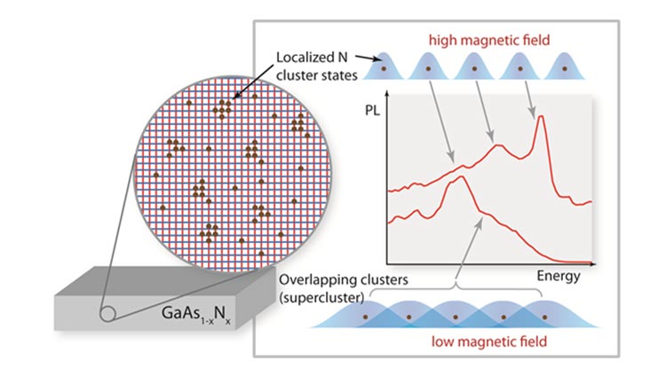
We use high magnetic fields to unravel the unusual behavior of electron traps in emergent PV materials. New insight into electron trapping in dilute nitride semiconductors will help mitigate undesirable transport properties so that these semiconductors can be used for ultra-high-efficiency solar cells.
Probing Direct-Indirect Crossover
We also use high magnetic fields to probe the nature of the direct-indirect crossover. For example, in studying AlGaAs, we have shown that the crossover behaves as an alloy-broadened first-order phase transition.
Strain in Semiconductors
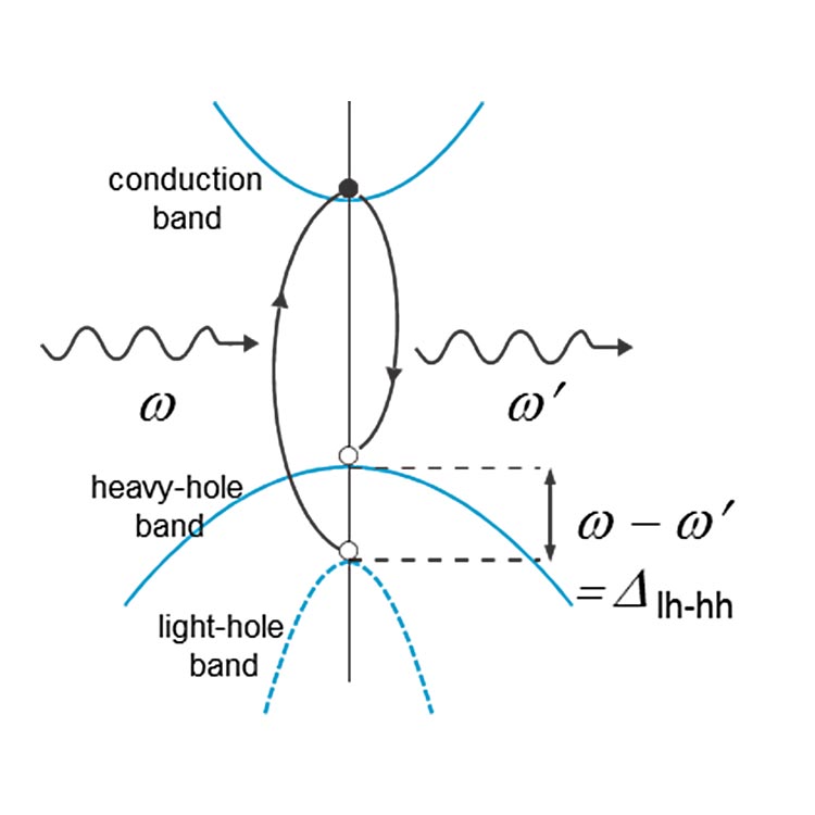
Using our novel ultra-sensitive probe for strain in semiconductors, we have observed a new light-hole to heavy-hole interband electronic Raman process in AlGaAs that has evaded discovery for almost half a century. This effect can be used to determine epitaxial strain-induced splittings in the band structure with unprecedented resolution.
Solid-State Lighting
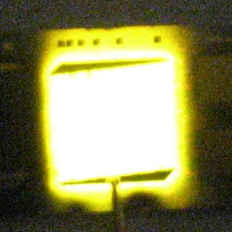
We are exploring high-bandgap III-phosphide alloys, such as AlInP, grown metamorphically on GaAs substrates, as candidate materials for amber LEDs. LED bulbs can create white light by combining discrete wavelengths from individual red, green, blue, and amber LEDs, an approach known as color-mixing. These bulbs have the potential for higher efficiencies and advanced color-tuning functionality compared to current bulbs. However, the lack of efficient green and amber LEDs has impeded progress in realizing such architectures.
Contact
Molecular Beam Epitaxy
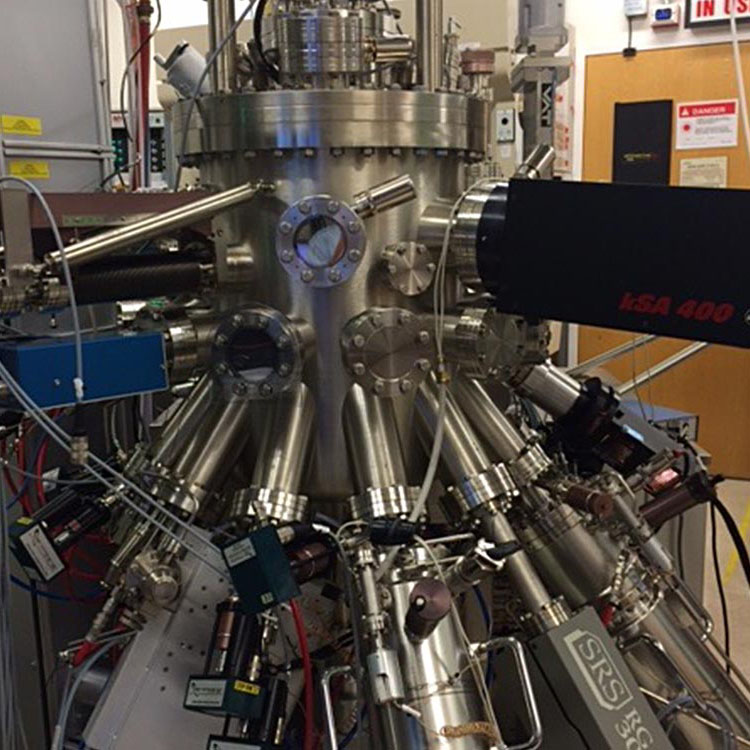
We use molecular beam epitaxy (MBE) to grow a variety of III-V and II-VI based semiconductors, including AlGaAs, GaAsBi, GaPBi, and ZnCdSe. We are also exploring the use of light stimulation of the growth surface, with the goal of overcoming limitations to the epitaxy of heavily doped semiconductors and heterovalent interfaces, as well as growth at low temperatures.
Contact
Micro-Photoluminescence Imaging
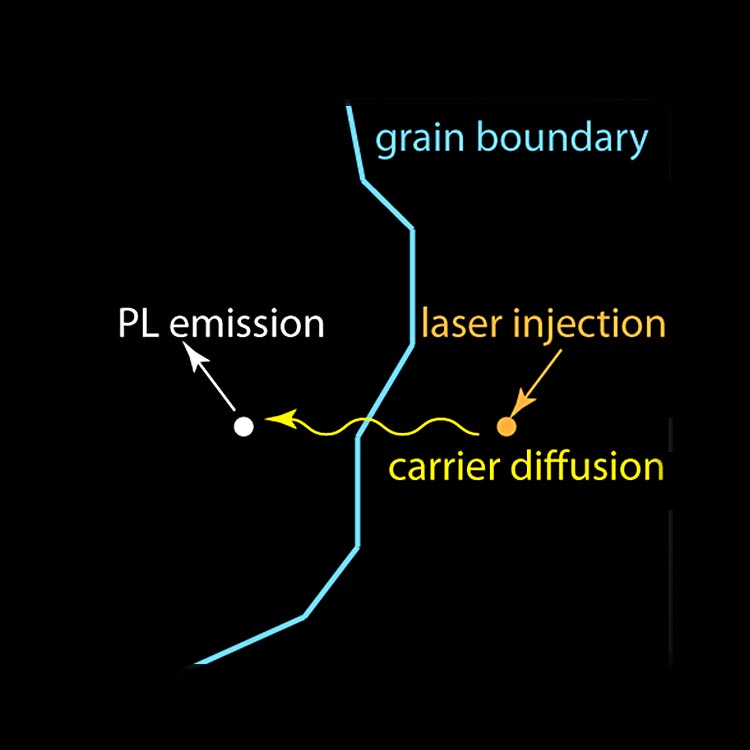
Understanding how defect states influence carrier transport in semiconductors is important for improving device performance, but most measurement techniques only provide this information indirectly. By decoupling the photon injection and collection optics, we can spatially resolve where carriers recombine in relation to where they are generated.
Carriers are photoinjected into a single location with a focused laser, while PL is simultaneously collected and imaged from a larger area. PL detected in neighboring regions of the material provides direct information about the distances and locations to which carriers have diffused. This new information can be used to guide the development of polycrystalline CdTe for improved solar cell performance.
We have also adapted this micro-PL imaging technique to include time resolution as well as spatial resolution. This approach has allowed us to determine how the carrier lifetime changes near extended defects.
Contact
Buildings Research
We apply advanced materials research techniques, such as the Materials Genome Initiative approach, to address key problems related to buildings energy use. Our key focus areas relate largely to the building envelope, which includes windows technologies and opaque components such as walls and roofing. We conduct research into responsive architectural materials that allow a building to change its properties based on existing environmental conditions to maximize energy savings.
Contact
Photovoltaic Module Soiling Mitigation and Thermal Control
Two large impacts on power generation by fielded PV modules are dust/soiling, which prevents light from getting to the absorber layer, and substantial heating of the modules when they are collecting energy. We perform systematic studies to understand the processes involved; for example, we seek to predict the effects of soiling for different environmental conditions.
We are working with the PV community to:
- Develop models that predict seasonal/annualized soiling losses at new PV plant sites
- Provide the PV industry with tools/knowledge for successful long-term deployment of modules with value-added antireflection and anti-soiling coatings
- Identify the most important physical and chemical adhesion mechanisms involved with dust particles adhering to PV module surfaces.
Contact
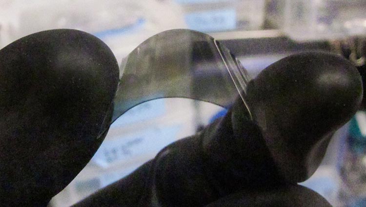
Transparent Window Insulation
We work on a number of technologies related to buildings, developing materials that may address the large installed windows retrofit market to substantially improve fenestration and building-envelope energy efficiency. We are developing transparent vacuum insulation films that use nano- to micrometer-sized vacuum capsules integrated with standard window plastics. They can be integrated with low-e coatings to mitigate infrared transmission and produce up to R-20 films only millimeters thick but transparent enough for window applications.
Contact
Theory and Computation
For electronic structure theory and computational materials science activities, we use computational methods to study energy materials from a theoretical perspective. We collaborate closely with other experimental materials science research groups to translate physical insights gained from computations into progress in developing real materials.
Contact
Contact
The Materials Science Center is part of the Materials, Chemical, and Computational Science directorate, led by Associate Lab Director Bill Tumas.
Share