Analytical Microscopy and Imaging Science
NLR's microscopy and imaging research develops analytical characterization, in-situ techniques, and multiscale workflows to evaluate the structure-property relationships, defects, and degradation mechanisms across energy technologies.
Tools include transmission and scanning electron microscopes, focused ion beam microscopes, scanning probes, and electro-optical imaging tools.
Core Competencies
NLR’s analytical microscopy and imaging science core competencies include structural and compositional mapping, interfacial properties, operando mechanisms, multiscale characterization, cryo/inert workflows, and autonomous workflows.
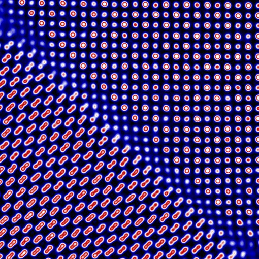
Many different types of signals and responses are produced when an electron beam interacts with a sample, including diffraction patterns, characteristic X-rays, and inelastic interactions. By scanning an electron beam across a sample and collecting information from these interaction phenomena, maps of sample characteristics can be generated with spatial resolutions down to the atomic scale.
Relevant Techniques
-
Structural mapping: Electron backscatter diffraction (performed in the scanning electron microscope (SEM)) and 4D-scanning transmission electron microscopy acquire diffraction patterns as a function of electron beam position to spatially map out structural details of the sample. The diffraction patterns are indexed and analyzed to provide spatially resolved information about crystalline phases, microstructure, and strain.
-
Elemental mapping: Energy-dispersive X-ray spectroscopy (EDS or EDX) provides spatially resolved maps of elemental composition by detecting characteristic X-rays generated by each element present in the sample. EDS can be performed in the SEM and transmission electron microscopy (TEM).
-
Chemical mapping: Electron energy loss spectroscopy (EELS, performed in the TEM) collects information about the chemical and bonding configurations of the elements in the sample by measuring the amount of energy lost by the primary electron beam as it interacts with the sample. EELS spectra can be analyzed to understand the sample composition, elemental oxidation state, and electronic structure.
Interfacial structure and chemistry are critical determinants of both performance and degradation in many devices. Microscopy can help reveal the structures and phases present at interfaces; the chemical bonding and oxidation states of interfacial species; and interfacial potentials or charge transfer behavior, as well as how all these features evolve under stimuli such as bias application or elevated temperature. Moreover, as interfaces are often highly heterogeneous, the ability to probe local structures, chemistry, and functional properties with high spatial resolutions enable correlated measurements that reveal fundamental structure-property relationships, as well as underlying mechanisms of key interfacial processes.
Relevant Techniques
-
Diffraction techniques: Electron diffraction in either the scanning electron microscope (using electron backscatter diffraction) or scanning transmission electron microscope (using 4D-STEM) can reveal phase coexistence or grain orientations at interfaces. 4D-STEM can also be used to map interfacial strain fields.
-
STEM spectroscopy: Energy-dispersive X-ray spectroscopy or electron energy-loss spectroscopy (EELS) in the STEM, enables elemental mapping at interfaces. EELS can furthermore reveal oxidation states and bonding structures of interfacial species.
-
Scanning probe microscopy: Scanning probe techniques such as Kelvin probe force microscopy or scanning spreading resistance microscopy can map interfacial potentials or local resistivity, respectively.
-
Cryogenic and inert workflows: As many interfaces are sensitive to air, moisture, and electron beam-induced damage, cryogenic and inert workflows are often essential to preserve delicate interfaces for artifact-free characterization.
Understanding of energy systems under operating conditions is valuable to identify the structure-property relationships when external influences (strain, bias, light, heat, field, and chemical environment) impact the system. Therefore, using analytical tools that can simultaneously image or probe the material/system while undergoing a reaction can help to identify the atomic-to-nanoscale mechanism. The electron microscopy tools have capabilities for high temperature, cryo, bias, light, controlled inert, and chemical environments. Scanning probe atomic force microscopy (AFM) is capable of inert environments, high temperature, and bias. Electro-optical imaging systems regularly use bias and light stimulus, though some can include more diverse external influences.
Relevant Research Areas
-
Ion transport: AFM, scanning transmission electron microscopy, scanning electron microscopy, and electro-optical tools can map ions at varied length scales.
-
Charge transport: Electrical measurements can be performed using various tools to identify low resistance pathways through materials and interfaces.
-
Chemical reactions: Introducing a second material or reactive element to a sample is possible to evaluate the surface, structural, or compositional changes (e.g., corrosion).
-
Transient states: During a material process or reaction, metastable phases in materials or intermediate states can be captured using high-resolution imaging, spectroscopy, and diffraction analysis.
-
Phase changes: Commonly during a change in temperature or composition, a phase change reaction can be imaged/mapped to understand how materials transform when triggered.
-
Annealing: Increasing the temperature at interfaces or with separated particles can cause annealing which can be captured at multiple length scales to observe the process.
-
Growth: Building layered material interfaces or formation of polymers can be overserved during curing to understand the epitaxy or uniformity of the process.
-
Defect formation/motion: Defects in materials commonly respond to an external stimulus, where the dynamics of these features can be traced with atomic-to-microscale resolution.
Multiscale characterization workflows are essential for understanding the structure, properties, and performance of energy materials. By combining characterization techniques that probe different length scales, we can gain insights into the fundamental processes governing energy conversion, storage, and transport. These workflows enable the development of novel materials with improved efficiency and durability.
Relevant Research Areas
-
Battery materials: Characterizing fundamental ion transport phenomena at the nanoscale can inform macroscale behavior that helps optimize energy density, rate capability, and cycle life of battery materials.
-
Solar cells: Understanding the morphology, crystal structure, and optoelectronic properties of photovoltaic materials across many length scales, from atomic interfaces to full-scale devices, is critical for improving light absorption, charge carrier transport, and device efficiency.
-
Energy storage: Characterizing the nanoscale and microscale mechanisms underpinning degradation observed in macroscale energy storage systems is vital for developing energy storage materials with both high storage capacity and long duration lifetimes.
Many materials experience degradation upon exposure to air, moisture, or electron beam irradiation. Cryogenic and inert workflows can protect these sensitive samples to enable artifact-free characterization. During inert transfers, samples are moved from glovebox storage to the microscope and back without air exposure. In cryogenic workflows, low temperatures (typically -150°C to -196°C, enabled by liquid nitrogen cooling) are used to stabilize sensitive materials, or sensitive states in materials, against electron beam-induced damage. These workflows can be combined with various analytical techniques to enable multimodal characterization.
Relevant Research Areas
-
Biological materials: Flash freezing of hydrated biological samples followed by cryogenic (scanning) transmission electron microscopy ((S)TEM) characterization enables determination of the three-dimensional structures of proteins, viruses, and other complexes.
-
Battery materials: Inert transfers prevent oxidation and surface degradation of reactive battery samples, while cryogenic (S)TEM reduces beam-induced damage to sensitive constituent materials, such as lithium-containing compounds.
-
Quantum materials: Cryogenic (S)TEM enables study of novel low-temperature structures in quantum materials, such as skyrmions or charge ordering.
-
Organic and hybrid materials: Cryogenic temperatures reduce beam-induced damage in many organic (e.g., polymers) and hybrid organic-inorganic (e.g., metal-organic frameworks, metal-halide perovskites) materials to enable high-resolution (S)TEM characterization.
The rise of autonomous electron microscopy is transforming materials characterization, enabling researchers to conduct experiments at an unprecedented scale, with enhanced reproducibility and intelligence. By leveraging the capabilities of artificial intelligence (AI) and machine learning (ML) algorithms, autonomous scanning transmission electron microscopy goes beyond the limitations of manual experimentation, allowing for the discovery of hidden features, accelerating materials discovery, and establishing more precise statistical models for materials and chemical systems.
In 2025, NLR is hosting the Autonomous Research for Real-World Science Workshop to bring together leading experts in materials science, chemistry, and autonomous experimentation to explore practical, real-world applications of autonomous research.
Unique Capabilities and Advancements
Novel control systems: We have developed unique, centralized microscope controllers that seamlessly integrate hardware and software components from multiple vendors, enabling precise and flexible control of the microscope.
Tailored ML solutions: We employ specialized ML algorithms designed specifically for the challenges of electron microscopy, such as few-shot learning for rapid and flexible image segmentation and classification, and predictive modeling for in-situ forecasting of chemical reactions.
Automated experimentation: AI/ML provides real-time guidance to the microscope, optimizing data collection, exploring regions of interest, and even conducting atomic-scale fabrication.
Contact
For general inquiries about the facilities, specialized capabilities/workflows, and additional contacts, please contact [email protected] or:
Share
Last Updated Dec. 7, 2025


