Electro-Optical Imaging
NLR's electro-optical imaging techniques provide spatial characterization of optoelectronic materials and devices. These versatile techniques can be applied to quickly obtain information from small devices to full-scale modules.
Photoluminescence
Photoluminescence (PL) imaging uses light excitation and collects luminescence from the semiconductor material as excess carriers transition from an excited state to the ground state. The intensity of the luminescence is proportional to material quality and the voltage that can be generated by the solar cell device.
Mapping PL intensity provides a spatially resolved assessment of material quality by displaying decreased intensity in areas containing defects, impurities, and poor surface and interface passivation. PL imaging can be applied to stages of solar cell manufacturing, from the bulk semiconductor in ingot, wafer, or as-deposited film forms, throughout processing steps, and to finished cells and module assembly.
Electroluminescence
Electroluminescence (EL) imaging uses electrical excitation in the form of applied voltage and current to drive excess carriers into the solar cell device. EL imaging is applied to metallized cells when contact can be made for injecting carriers. EL images show material quality and excess carrier lifetime as PL does, but EL images are also sensitive to how carrier injection can be affected by series resistance of the conductive structures.
EL imaging can also be induced optically in a finished cell using patterned illumination and imaging, and this technique can be referred to as light-induced EL or contactless EL. Voltages are induced by light in a partially illuminated pattern of a cell, and this voltage spreads and induces EL in the dark patterned areas of the same cell. In the field, EL-equivalent images can be collected with optical excitation which avoids the need to disconnect the module cables.
Dark Lock-In Thermography
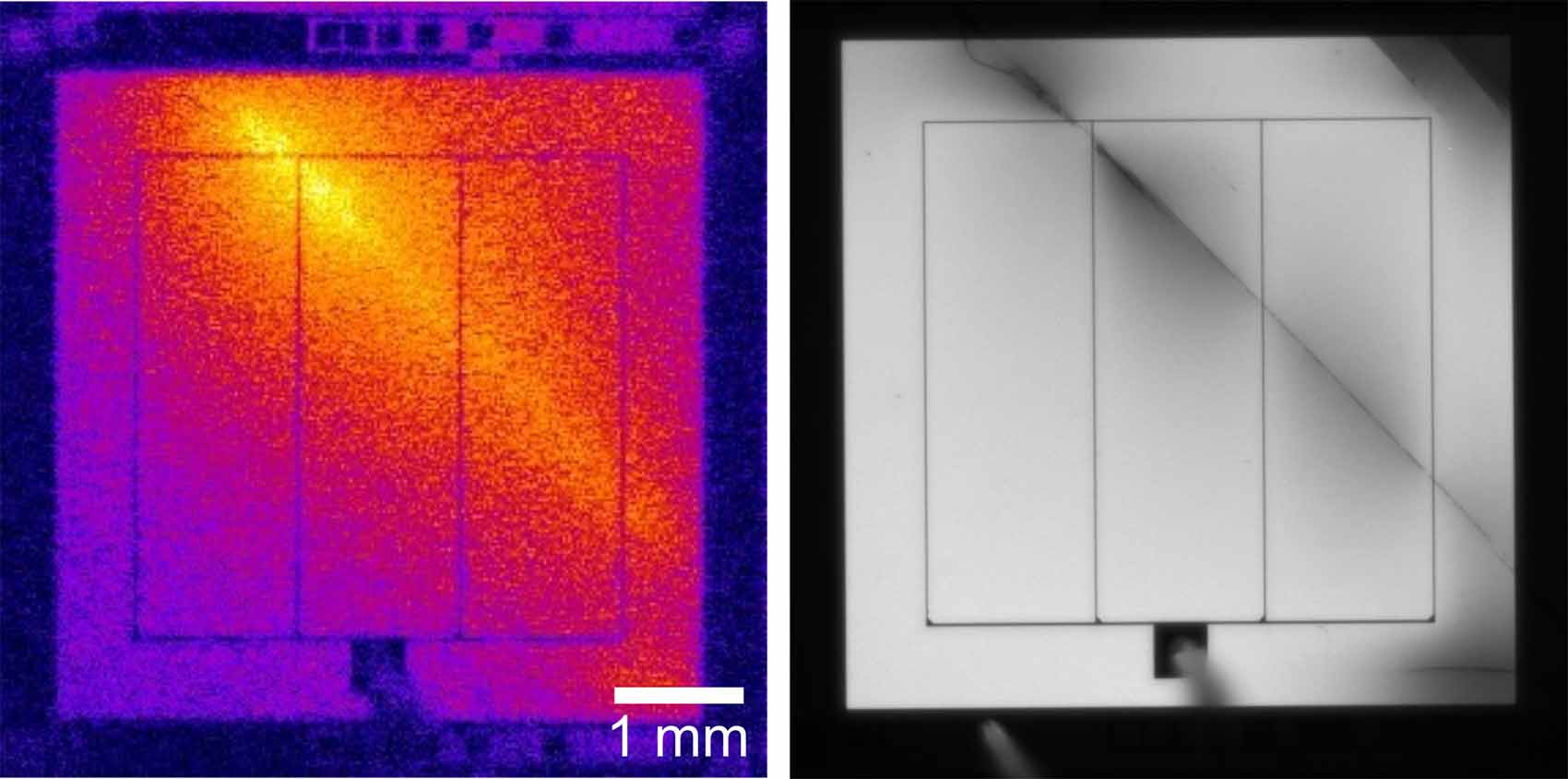
Dark lock-in thermography (DLIT) is an imaging technique that provides spatial characterization of heat and is used to identify areas of a solar cell or module where heat is generated through carrier recombination, shunts, and series resistance. DLIT can be a powerful technique to identify current losses in localized defects in solar cell devices.

DLIT image (left) and associated EL image (right) showing an electrical shunting pathway associated with a crystalline defect running across a photovoltaic device.
Deep-Level Transient Spectroscopy
Deep-level transient spectroscopy (DLTS) is a sensitive technique for characterizing defect states within the semiconductor material of a solar cell device. Capacitance transients occur when majority and minority carriers can become trapped in defect states as the device's depletion width is toggled back and forth with applied bias. When collecting and analyzing capacitance transients as a function of time and temperature, an Arrhenius plot of the data can give defect state activation energies within the bandgap.
DLTS can characterize defect levels by measuring their concentration, energy level, and capture cross section. Because the baseline capacitance of the solar cell device under test is based on semiconductor doping, the sensitivity of detecting defect levels is a fraction of this doping such that defect concentrations as low as ~1011 cm-3 may be observed for typical doping levels of ~1016 cm-3.
Contact
Share
Last Updated Dec. 6, 2025
