Transmission Electron Microscopy
NLR uses transmission electron microscopy (TEM) tools and techniques, allowing researchers to image and characterize materials down to the atomic level.
There are two main types of TEM—conventional TEM and scanning TEM (STEM)—each with its own strengths. Often, a combination of these techniques is used to gain a wealth of information about the structure, composition, and properties of your material.
Conventional Transmission Electron Microscopy
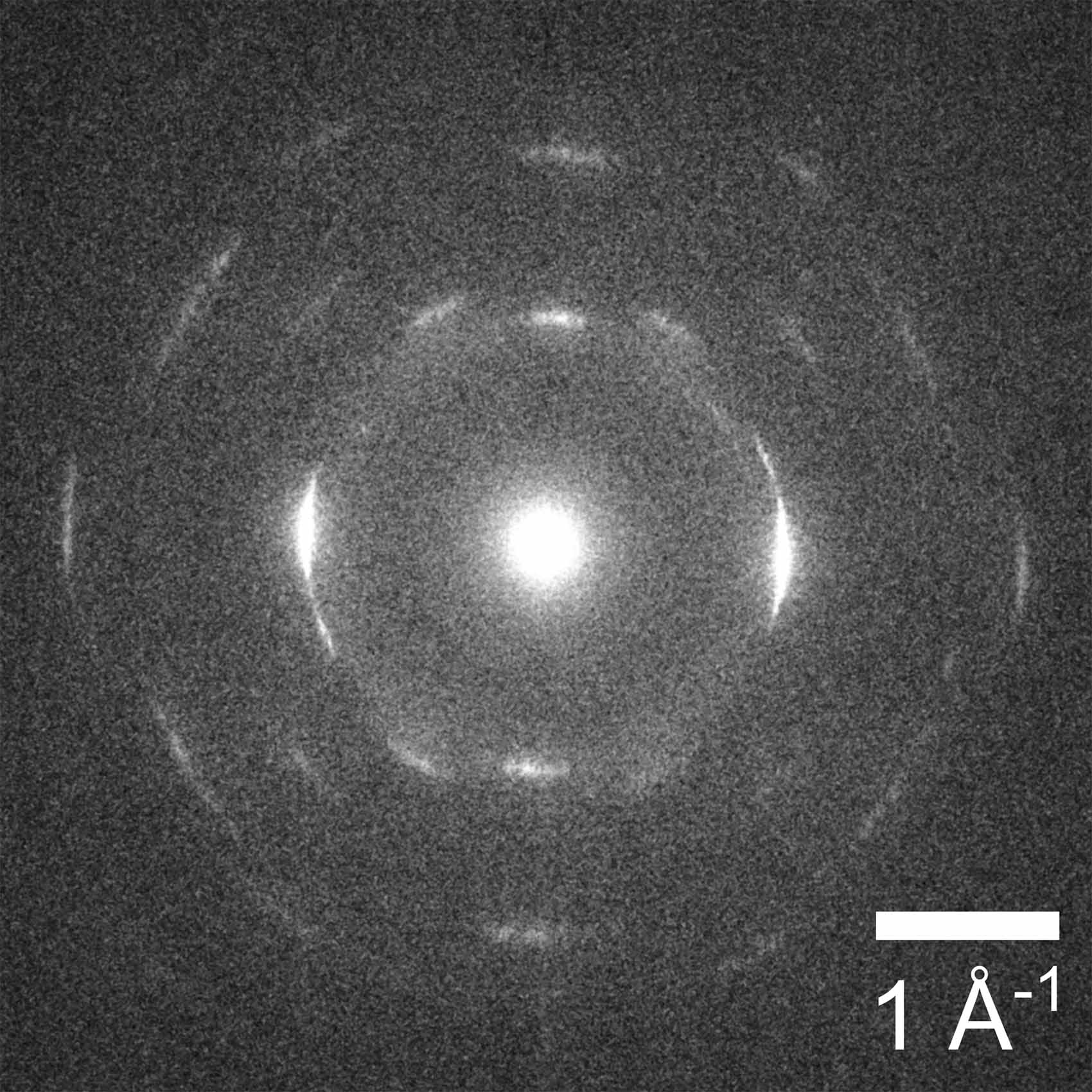
Selected area electron diffraction pattern of a Wurtzite structured thin film.
In conventional TEM, a beam of high-energy electrons is transmitted through an incredibly thin sample (often less than 100 nm) of your material. As the electrons pass through, they are scattered depending on the structure and composition of the specimen. An image or diffraction pattern is then formed on the camera that reveals specific information about your specimen.
Common uses:
- Observing the morphology (shape and size) of nanoparticles
- Identifying defects like dislocations and grain boundaries
- Studying crystal structure and lattice arrangements
- Measuring diffraction from nanoscale volumes (selected area electron diffraction)
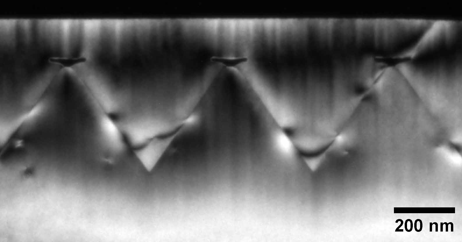
Dark-field TEM image of dislocations formed at a lattice-mismatched interface of a gallium phosphide film grown on a V-grooved silicon substrate.
Scanning Transmission Electron Microscopy
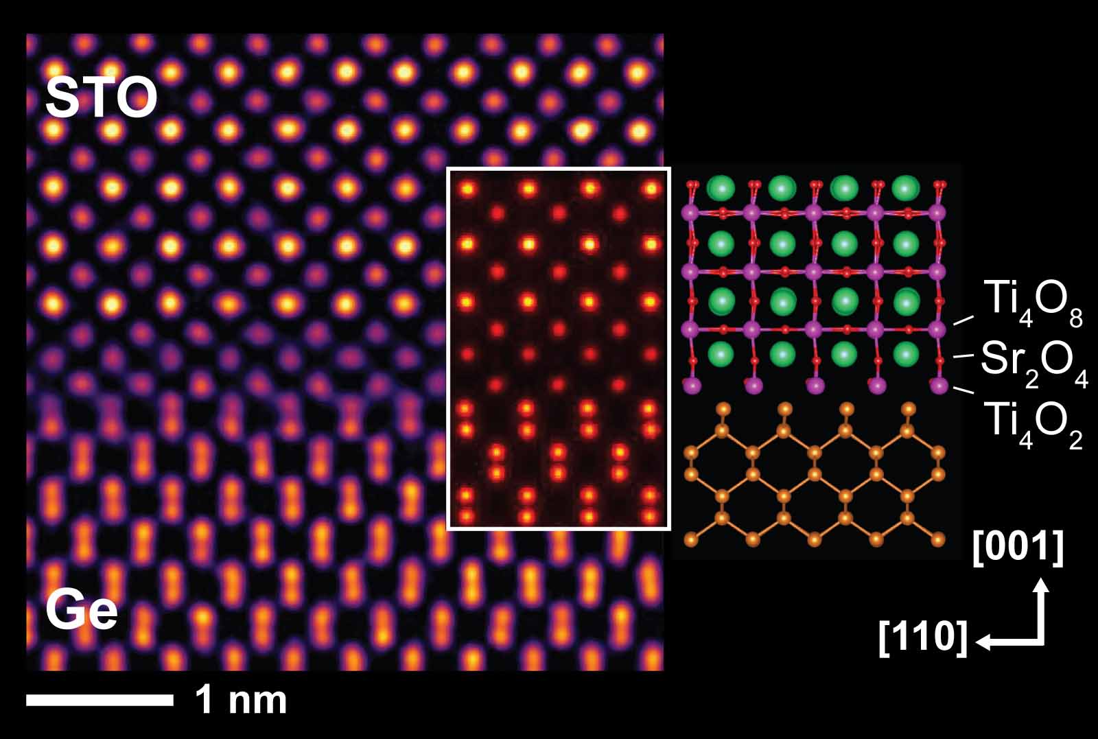
High-resolution STEM imaging of oxide and semiconductor interfaces reveals changes in bonding and structural rearrangement that directly informs processing.
In STEM, the electron beam is focused down to a probe and scanned across the sample in a line-by-line fashion. Collecting the transmitted electrons at each point builds up an image using a variety of detectors that take advantage of different contrast mechanisms to provide information about the sample's structure. STEM offers the advantage of collecting additional spatially resolved information beyond just the image, such as the elemental composition of specific regions within the sample.
Common uses:
- High-resolution imaging of materials down to the atomic level
- Elemental and chemical analysis using techniques like energy-dispersive X-ray spectroscopy (EDS) and electron energy loss spectroscopy (EELS)
- Interfacial characterization between different materials
Techniques
Energy-dispersive X-ray spectroscopy (EDS or EDX) is an analytical technique used for the elemental characterization of a sample. It works by detecting the characteristic X-rays emitted from a specimen when it is bombarded with high-energy electrons. Key principles include:
-
X-ray emission: When a high-energy electron beam interacts with the atoms in the sample, it can eject inner-shell electrons. The vacancies left by these ejected electrons are filled by electrons from higher energy levels, resulting in the emission of X-rays with characteristic energies specific to each element.
-
X-ray detection: These characteristic X-rays are detected by an EDS detector, which measures their energies and intensities to identify and quantify the elements present in the sample.
EDS is typically combined with either scanning electron microscopy or STEM imaging to perform elemental mapping from the microscale all the way down to atomic resolution.
Common Uses
-
Elemental mapping: By scanning the electron beam across the sample and detecting the emitted X-rays at each point, an elemental map can be created, showing the spatial distribution of elements within the sample.
-
Quantitative analysis: EDS can provide quantitative information about the elemental composition of a sample, including the relative concentrations of different elements.
-
Phase identification: EDS can be used to identify different phases or compounds within a sample by their unique elemental signatures.
-
Nanomaterials research: STEM-EDS is extremely useful for characterizing the composition and distribution of elements in nanoparticles, thin films, and other nanostructures.
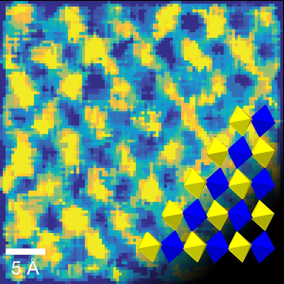
Atomic-resolution STEM-EDS mapping reveals the emergence of cation ordering at the atomic level, informing synthesis pathways and emergent properties.
Electron energy-loss spectroscopy (EELS) is a technique used in TEM to analyze the energy losses of electrons as they interact with a sample, which are characteristic of the sample's elemental composition, chemical bonding, and electronic structure. Combining STEM with EELS allows for spatial mapping of these material characteristics down to the atomic scale.
Common Uses
- Chemical composition: EELS can identify the elemental composition of nanoscale regions within a sample. It is particularly useful for analyzing light elements that are difficult to detect with other techniques.
- Chemical bonding: By examining the fine structure of EELS spectra, chemical bonding states (such as oxidation states) and electronic structure can be analyzed.
- Surface plasmon resonance: EELS can probe surface plasmons, which is valuable for studying nanoparticles, catalysts, and other nanostructured materials.
- Thickness mapping: EELS can be used to measure the thickness of thin films or biological samples by analyzing the intensity of energy-loss peaks.
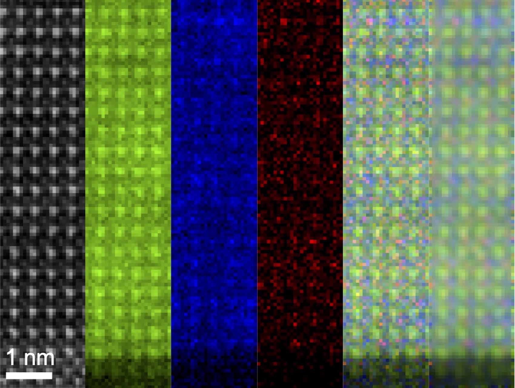
STEM-EELS mapping image STEM-EELS mapping of core loss signals provides valuable insight into composition and intermixing at interfaces that inform processing pathways.
Four-dimensional scanning transmission electron microscopy (4D-STEM) is a versatile electron microscopy technique that combines the high spatial resolution of STEM with the information-richness of electron diffraction. In 4D-STEM, the electron beam is scanned across a specimen, capturing a diffraction pattern at every point, with spatial resolution down to the atomic scale. This produces a 4D-STEM dataset that can then be analyzed to reveal a multitude of nanoscale characteristics, such as crystalline structure, phase heterogeneity, nanoscale strain, and even internal electric fields.
Common Uses
- Crystal phase and orientation mapping: Analyze the nanoscale crystalline phases and microstructure within your material.
- Strain mapping: Understand how your material deforms and responds to external forces at the nanoscale.
- Virtual imaging: Generate a variety of STEM images (e.g., bright-field, dark-field) and diffraction patterns all from the same 4D-STEM dataset to visualize unique features in your specimen.
- Differential phase contrast imaging: Map out electric and magnetic fields in your specimen with nanoscale spatial resolution.
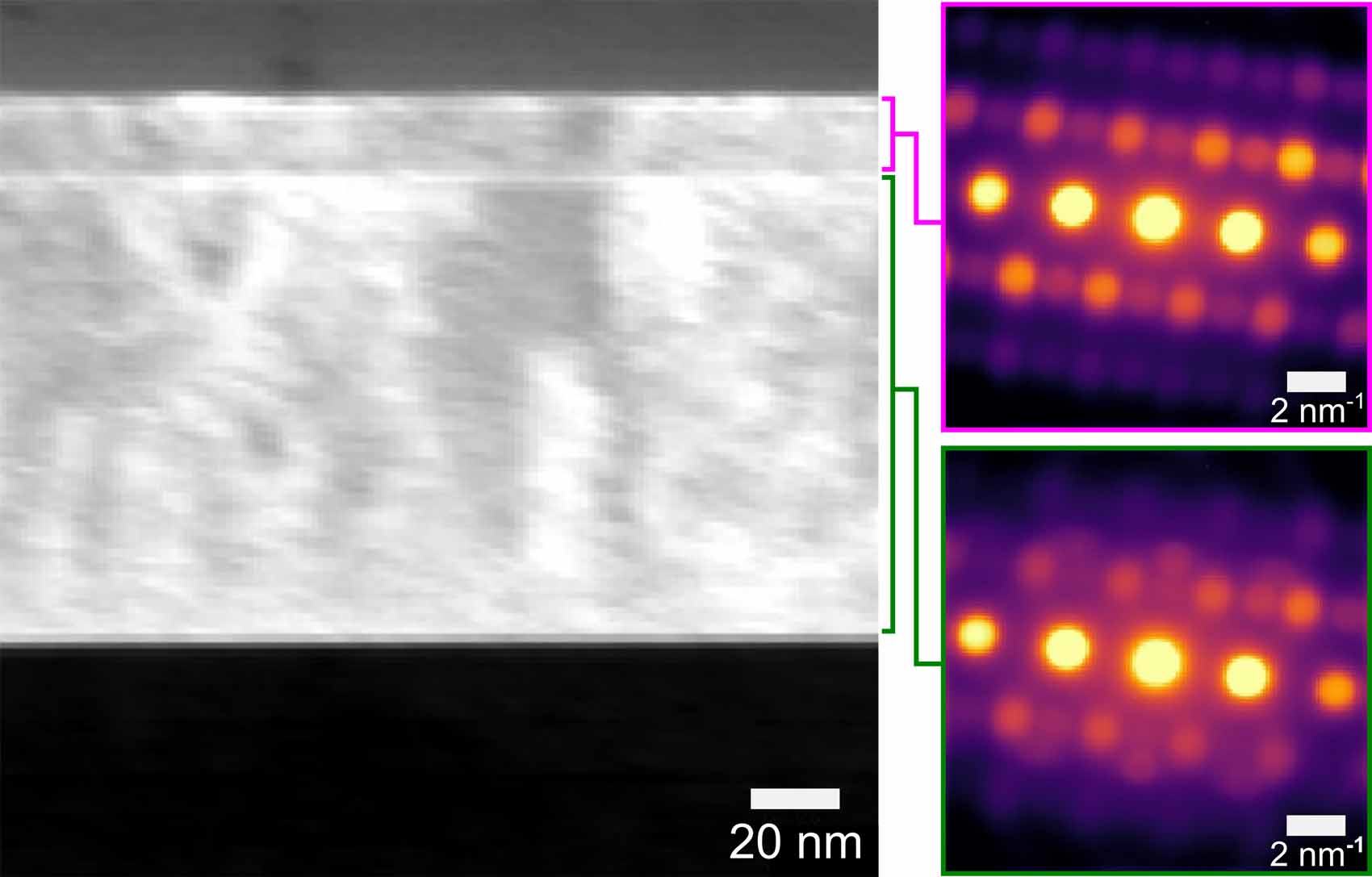
4D-STEM dataset of a multilayer, thin-film system displaying virtual selected area electron diffraction patterns extracted from two individual thin-film layers.
Tools
Contact
Share
Last Updated Dec. 6, 2025
