Cadmium Telluride Solar Cells
The United States is the leader in cadmium telluride (CdTe) photovoltaic (PV) manufacturing, and NREL has been at the forefront of research and development in this area.
PV solar cells based on CdTe represent the largest segment of commercial thin-film module production worldwide. Recent improvements have matched the efficiency of multicrystalline silicon while maintaining cost leadership.

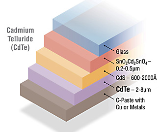
CdTe-based PV is considered a thin-film technology because the active layers are just a few microns thick, or about a tenth the diameter of a human hair. A schematic of a typical CdTe solar cell is shown here. Transparent conducting oxide (TCO) layers such as SnO2 or Cd2SnO4 are transparent to visible light and highly conductive to transport current efficiently. Intermediate layers such as CdS help in both the growth and electrical properties between the TCO and CdTe. The CdTe film acts as the primary photoconversion layer and absorbs most visible light within the first micron of material. Together, the CdTe, intermediate, and TCO layers form an electric field that converts light absorbed in the CdTe layer into current and voltage. Metal is placed on the back to form electrical contacts. In production, all these layers are deposited on incoming glass and processed into complete solar panels in just a few hours.
Our Expertise
NREL has a world-class assembly of CdTe photovoltaic research tools and expertise. This includes the ability to deposit all the layers mentioned above as well as novel materials and device structures. Our work also includes advanced characterization, device modeling, and collaboration with university and industry partners.
Research Areas
We are working with single crystals, large grains, and standard cells to understand and push the limits of CdTe. Efforts include:CdTe is generating electricity at levelized costs that are less than or equal to traditional fossil-fuel energy sources, and it has headroom for improvement. Standard polycrystalline absorber layers have short aggregate carrier lifetimes of a few nanseconds and low doping relative to other solar cell materials. Our work focuses on improving these material properties to increase voltage, diode quality, and efficiency. Resolving these issues requires addressing big materials science challenges with a combination of innovation, synthesis, characterization, and fundamental scientific understanding.
- Learning the art of doping on single-crystal material and transferring to polycrystalline material
- Quantifying the role of defects, surfaces, and grain boundaries
- Advancing our understanding through theoretical calculations and characterization.
Realizing the benefits of higher CdTe lifetime and doping will require high-quality interfaces. So, in parallel, we are studying surface and interface defects and developing passivation strategies to minimize interface recombination. In addition to improving the voltage and diode quality, improved interfaces can maximize transmission to increase current and can remove impurities to increase reproducibility and stability.
These projects, together with other CdTe research efforts, are designed to benefit established CdTe manufacturers as well as new start-ups by improving CdTe photovoltaic performance, reducing costs, and advancing fundamental knowledge.
Tools and Capabilities
NREL has a range of tools and capabilities available for R&D in CdTe materials and devices, including:

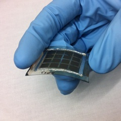
Flexible CdTe solar cells on ultrathin glass (Mahabaduge et al.)
- TCO layers
- SnO2 by metal-organic chemical vapor deposition
- SnO2, Zn2SnO4 alloys by sputtering
- In2O3, ZnO, Zn2SnO4, and Cd2SnO4 by reactive sputtering
- High-permittivity alloys
- SnO2:ZnO, CdO, and CdO:SnO2 alloys by metal-organic chemical vapor deposition
- Buffer and CdS layers
- Chemical-bath deposition
- Reactively sputtered CdS:O
- CdTe layers – close-spaced sublimation
- Co-evaporation for CdZnTe and CdMgTe
- Molecular-beam epitaxy of CdTe and other II-VI compounds
- CdCl2 treatments
- Wet process (CdCl2 + methanol or H2O)
- Dry process, close-spaced sublimation
- Back contacts
- Wet process (chemical pre-treatments + HgTe -doped graphite)
- Dry process (ion-beam treatment + ZnTe:Cu/Ti)
- Alternative contact processes such as Cu/Au, CuTe, and SbTe
- Alternative device structures
- Ultrathin glass
- Flexible devices
- Substrate device
- Stability measurements and interpretation
- Characterization by scientists
- Lifetime, Hall, accelerated lifetime testing, current-voltage (I-V), DLTS, capacitance, secondary ion mass spectrometry, Auger electron spectroscopy, X-ray photoelectron spectroscopy, cathodoluminescence, photoluminescence, transmission electron microscopy, electron backscatter diffraction, X-ray diffraction, inductively coupled plasma, and other measurements
- Collaborations with NREL computational scientists
- CdTe ab-initio density functional theory calculations, device simulation, and advanced measurement simulations.
Contact
Matt Reese
Researcher IV, Physics
Share

