Hybrid Tandem Solar Cells
NREL is investigating several hybrid tandem solar cell projects that build on a silicon platform and aim to provide viable prototypes for commercialization.
To achieve aggressive cost reductions in photovoltaics (PV) beyond the 6¢/kWh SunShot Initiative 2020 goal, module efficiency must be increased beyond the single-junction limit. Many device architectures have been investigated, but successful devices will likely use industry's standard platform—crystalline silicon.
Our research falls into two categories:
- Epitaxial devices grown monolithically on Si
- Mechanically stacked devices, where a top cell is fabricated separately and then attached to a Si bottom cell.
Tandem-junction cell architectures present a path toward higher module efficiencies over single-junction designs because of the ability to split the solar spectrum into multiple bands that can be more efficiently converted by separate devices. This enables surpassing the limiting efficiency of single-junction Si (~29%), which has neared its theoretical limit. As module costs drop, balance-of-systems costs dominate the cost of PV installations, and gains in efficiency become a more powerful lever to influence overall system costs. These higher-efficiency tandem modules may also enable low-concentration PV installations using single-axis tracking.
This research leverages our research and development programs in high-efficiency III-V multijunction PV, low-cost III-V PV, and silicon solar cells.
Our Expertise
We have expertise in:
- Heteroepitaxial growth of III-Vs on Si
- Fabrication of high-quality n-type Czochralski Si bottom cells optimized for use in tandems
- Wafer bonding
- Mechanical stacking
- Transparent, conductive adhesives for cell stacking
- Three-terminal device designs
- Substrate removal techniques for III-V lift-off
- Tandem device modeling (Sentaurus)
- Electronic structure calculations of material properties and defects
- Development of new top-cell materials (epitaxial growth and combinatorial physical vapor deposition)
- Nanoimprint lithography
- Photoelectrochemical characterization
- Calibrated testing of multijunction solar cells (current density, voltage, quantum efficiency).
Research Areas
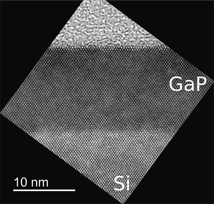
Transmission electron microscope image of epitaxial GaP on Si without antiphase domains.
Epitaxial Monolithic Tandems on Silicon
NREL has a long history of leadership in epitaxial tandem cells on Si, including more than a decade of developing lattice-matched dilute-nitride top-cell materials on Si and metamorphic GaAsP on Si tandems. More recently, we have perfected a method of preparing the Si surface for III-V epitaxy using an in-situ AsH3 etch in the metal-organic chemical vapor deposition (MOCVD) reactor before growth. This step quickly and efficiently cleans the Si surface of contaminants and establishes a double-step structure necessary for high-quality nucleation of polar materials (such as GaP and GaAs) on nonpolar Si. Lattice-matched GaP can then be grown directly on Si without forming antiphase domains, as shown in the transmission electron microscope image.
A second challenge facing III-V/Si epitaxy is lattice mismatch between Si and appropriate III-V top-cell materials such as GaInP2 or GaAsP. We use inexpensive nanoimprint lithography to pattern passivated Si bottom cells, then grow lattice-mismatched III-V materials using selective-area growth (SAG). Defect density in mismatched materials can be reduced by using aspect-ratio trapping, where angled defects terminate at interfaces, and small feature sizes, where defects are less likely to form. The nanoheteroepitaxy approach eliminates expensive graded buffer layers, enabling high-efficiency multijunction solar cells at lower cost. Our ultimate goal is low-cost triple-junction III-V/Si solar cells with potential efficiency >30%.
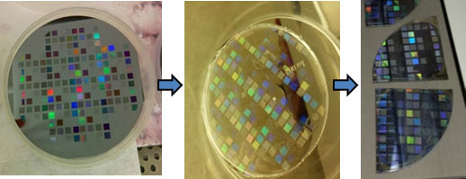
A silicon master (left) is used to produce a PDMS stamp (middle), which then leads to patterned sol-gel silicon dioxide on silicon (right).
We use substrate-conformal nanoimprint lithography as an inexpensive, scalable way to pattern nanoscale features on Si substrates. A master—which can be re-used many times—is made using more expensive techniques, such as electron-beam lithography or deep-ultraviolet lithography. Then, a mold is made using polydimethylsiloxane (PDMS) to replicate the pattern. Si samples, coated in a sol-gel SiO2 precursor film, are then "stamped" with the PDMS mold, resulting in SiO2 films on Si with nanoscale patterns. GaAs can then be grown selectively in the nanoscale features.
The benefits of this approach include:
- Large areas are possible using a roll-to-roll process
- Small features are possible, down to 10 nanometers
- The PDMS mold can conform to non-planar surfaces
- The sol-gel "resist" layer forms a dielectric that can become part of final device, for a streamlined process
- The master and stamps may be re-used many times.
Although III-V materials may provide the highest efficiency for tandem PV on Si, we are also investigating new materials that are less expensive. ZnSiP2, in particular, is a promising material for an epitaxial top cell, because it is lattice matched to Si and has a wide bandgap (2 eV). We have investigated the fundamental properties of ZnSiP2 using bulk single crystals grown using a flux technique. Using photoelectrochemical measurements, we observe high open-circuit voltage, indicating excellent material quality and potential for PV applications. Density functional theory calculations further establish ZnSiP2 as a "defect-tolerant" material, where the most favorable point defects form only shallow states that do not reduce performance significantly. Current work is focused on optimizing epitaxial growth of ZnSiP2 on Si for tandem PV applications.
Bonded and Stacked Tandems
Although monolithic tandems offer the most streamlined fabrication techniques, the efficiency of these epitaxially grown tandems has consistently lagged behind bonded and stacked tandems since it's possible to grow higher-quality material on a lattice matched substrate compared to directly on Si. Thus, we are working on bonded gallium indium phosphide (GaInP2) on Si tandem cells and comparing two-, three-, and four-terminal device configurations, as well as a voltage-matched approach discussed below.
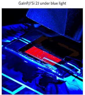
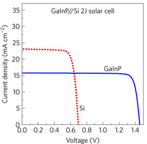
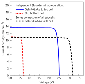
NREL-certified record efficiency III-V//Si mechanically stacked solar cells. In this four-terminal configuration, each cell is measured separately, and the efficiencies sum to 32.5% (GaInP//Si), 32.8% (GaAs//Si) and 35.9% (GaInP/GaAs//Si) under one-sun conditions.
In collaboration with the Swiss Center for Electronics and Microtechnology, we have fabricated several record-efficiency four-terminal tandem cells. For two junctions, we have reached 32.8% for GaAs//Si and 32.5% for GaInP//Si. For a triple junction, our record device efficiency is 35.9%. All of these cells are 1 cm2 and measured under AM1.5G illumination. These cells used our state-of-the-art III-V top cells, which operate close to their radiative limits, along with a specially designed Si heterojunction cell from the Center for Electronics and Microtechnology. The four-terminal configuration ensures that the efficiency can be extremely high, even without current matching.
To further improve bonded III-V on Si tandem cells, we have developed a transparent conductive adhesive bonding layer, which will enable two- or three-terminal operation of these devices. These adhesives eliminate the ultra-clean, smooth surfaces needed for direct wafer bonding, and they are compatible with textured Si, enabling enhanced light trapping and lower processing costs. We are using device modeling to evaluate multi-terminal device architectures, balancing the enhanced energy yield of multi-terminal approaches with the reduced power electronics requirements of simpler two-terminal devices. We aim to develop a Si-based tandem cell that will reach efficiencies >30% and create a viable economic pathway to meet SunShot's goals for levelized cost of energy. These tandems could also reach the SunShot price targets at 5- to 20-suns concentration to enable the low-concentration PV market, an emerging area without established contenders for optimal solar cells.
Voltage-Matched Hybrid PV Tandems
More generally, mechanical stacking permits the integration of many different PV technologies into multijunction solar cells because the sub-cells can be processed separately under optimal conditions before being integrated at the module level. We are exploring the use of voltage-matched module designs for mechanically stacked tandems that are amenable to two-terminal operation.
In such an architecture, strings of serially connected sub-cells defined within a top junction and strings of serially connected sub-cells defined within a bottom junction are separated by a transparent, electrically insulating intermediate layer. The strings are connected in parallel at each terminal. This approach has the potential to overcome long-standing challenges associated with integrating PV technologies in conventional current-matched architectures:
- No tunnel junctions are needed between stacked cells, which can be difficult to form between polycrystalline materials
- The sub-cell geometries do not have to be constrained to achieve current-matched conditions.

Schematic of a GaInP/Si voltage-matched tandem module.
In collaboration with the Naval Research Laboratory and Applied Novel Devices, we are developing voltage-matched tandem modules out of gallium indium phosphide (GaInP2) stacked on Si. Experimental demonstration of these modules are combined with cell- and module-level device modeling to assess their potential performance. We are also exploring the possibility of combining other PV materials, such as CdTe on Si and CdTe on CIGS.
Tool and Capabilities
Our tools and capabilities available for R&D in hybrid tandem solar cells include:
- III-V growth capabilities including metal-organic vapor-phase epitaxy (MOVPE), molecular-beam epitaxy (MBE), and hydride vapor-phase epitaxy (HVPE)
- Deposition of nontraditional semiconductors by MBE, CVD, and combinatorial PVD
- Si bottom-cell processing for up to 156 mm samples, including diffusion doping, oxidation, cleaning, deposition of passivated contacts
- Standard device processing capabilities including antireflection coatings, metallization, photolithography
- Wide variety of material and device characterization facilities (see Measurements and Characterization)
- Sentaurus device modeling.
Contact
Share

